CBSE Class 12-science Answered
22. Give reasons for the following:
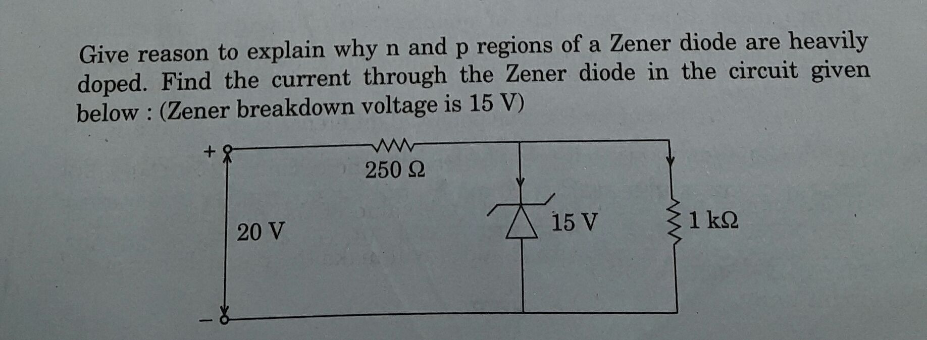
(i) The Zener diode is fabricated by heavily doping both the p and n sides of the junction
(ii) A photodiode, when used as a detector of optical signals is operated under reverse bias.
(iii) The band gap of the semiconductor used for fabrication of visible LED’s must at least be 1.8 eV.
Section
Asked by Malavika Umesh | 19 Feb, 2015, 12:25: AM
(i) Zener diode is fabricated to operate in reverse breakdown voltage region. It is designed to get a reduced breakdown voltage called zener voltage. This can be done by changing the thickness of depletion region to which the voltage is applied. This is achieved by doping heavily both the p and n side of p-n juction.
Kindly ask the other questions as seperate seperate query:
Answered by Jyothi Nair | 19 Feb, 2015, 12:12: PM
Concept Videos
-
Applications of p-n Diode - Part 1
 This video explains the diode in a forward and a reverse bias.
 -
PN diode application
 Diode V-I characteristics Diode as a rectifier Special purpose diodes.
 -
Applications of pn Diode
 Diode V-I characteristics Diode as a rectifier Special purpose diodes
CBSE 12-science - Physics
Asked by abhitailor158 | 06 Mar, 2019, 05:56: PM
CBSE 12-science - Physics
Asked by vk335548 | 05 Mar, 2019, 10:32: PM
CBSE 12-science - Physics
Asked by bjayanta | 05 Mar, 2019, 02:35: PM
CBSE 12-science - Physics
Asked by shariefy0007 | 22 Feb, 2019, 10:51: PM
CBSE 12-science - Physics
Asked by rohitraman1115 | 21 Nov, 2018, 04:57: PM
CBSE 12-science - Physics
Asked by Topperlearning User | 19 Jun, 2014, 01:54: PM
CBSE 12-science - Physics
Asked by Topperlearning User | 19 Jun, 2014, 02:06: PM
CBSE 12-science - Physics
Asked by Topperlearning User | 19 Jun, 2014, 02:11: PM
CBSE 12-science - Physics
Asked by Topperlearning User | 04 Jun, 2014, 01:23: PM
CBSE 12-science - Physics
Asked by Topperlearning User | 04 Jun, 2014, 01:23: PM