CBSE Class 12-science Answered
explain pnp and npn transistor
Asked by Sourav Jha | 06 Feb, 2015, 08:09: AM
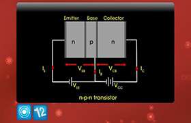
A PNP transistor is obtained by sandwiching a thin block of N-type semiconductor in between two blocks of P-type semiconductor. A thin block of P-type semiconductor sandwiched in between two blocks of N-type semiconductor forms a NPN transistor. The three sections of the transistor are emitter (E), base (B) and collector (C).
The emitter region is heavily doped and its size is moderate. The emitter supplies a large number of majority carriers for the current flow. The base region is very thin and lightly doped. Base region is in between the emitter and collector region. The collector region is moderately doped and larger in size than the emitter. The collector collects the majority carriers supplied by the emitter. The emitter and collector regions cannot be interchanged.
When a transistor is connected in a circuit, the base-emitter junction is always forward biased and the base-collector junction is always reverse biased.
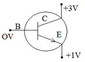
Working of PNP transistor:
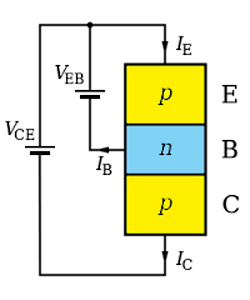
In the given PNP transistor circuit, the emtter-base junction is forward biased and hence, large number of holes flow from the emitter region to the base region. This causes the emitter current (IE). When the holes diffuse into the base region, only a few holes combine with electrons. The base region is very thin and lightly doped and has a low number density of electrons. Thus, a very small current flows through the base region called the base current (IB). The remaining holes reach the collector under the influence of the negative collector voltage. This produces a current in the collector region called the collector current (IC).
Thus, the emitter current is the sum of the collector current and the base current.
i.e. IE=IC+IB
Working of NPN transistor:
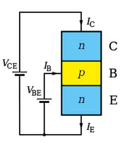
In the given NPN transistor circuit, the emitter-base junction is forward biased therefore, the electrons from the emitter diffuse into the base region producing the emitter current (IE). Since base region is very thin and lightly doped, so only about 5% of the electrons entering the base region recombine with the holes in the P region and this causes the base current (IB). Most of the electrons diffuse into the collector region and they are attracted by the positiove potential of the collector. Thus, the collector current (IC) flows.
Therefore, here also the emitter current is the sum of the collector current and the base current.
i.e. IE=IC+IB
In both the type of transistors, the collector current and the emitter current are of the order of milli-amperes while the base current is of the order of micro-amperes.
Answered by Faiza Lambe | 09 Feb, 2015, 10:02: AM
Concept Videos
-
Transistors - Part 1
 This video explains the types of transistors and its action.
 -
Transistors - Part 2
 This video explains the action of a transistor in detail.
 -
Transistors - Exam Decoded
 This video contains practice questions on a transistor.
CBSE 12-science - Physics
Asked by Topperlearning User | 04 Jun, 2014, 01:23: PM
CBSE 12-science - Physics
Asked by Topperlearning User | 23 Jun, 2014, 11:08: AM
CBSE 12-science - Physics
Asked by Topperlearning User | 10 Jul, 2014, 10:25: AM
CBSE 12-science - Physics
Asked by Topperlearning User | 23 Jun, 2014, 02:16: PM
CBSE 12-science - Physics
Asked by Topperlearning User | 14 Nov, 2014, 07:38: AM
CBSE 12-science - Physics
Asked by Topperlearning User | 10 Jul, 2014, 11:09: AM
CBSE 12-science - Physics
Asked by Topperlearning User | 04 Jun, 2014, 01:23: PM
CBSE 12-science - Physics
Asked by Topperlearning User | 04 Jun, 2014, 01:23: PM
CBSE 12-science - Physics
Asked by Topperlearning User | 23 Jun, 2014, 02:11: PM
CBSE 12-science - Physics
Asked by Topperlearning User | 10 Jul, 2014, 01:13: PM