Class 12-science H C VERMA Solutions Physics Chapter 23 - Semiconductors and Semiconducting Devices
Semiconductors and Semiconducting Devices Exercise 419
Solution 1
We know ,
![]()
![]()
![]()
And no. of atoms is given as :
![]()
![]()
![]()
Total no. of states = 2n
![]()
![]()
Total no. of empty
states =![]()
Solution 2
In case of pure semiconductor,
No. of electrons = No. of holes
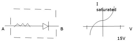
![]()
Also,
![]()
![]()
![]()
![]()
And from 1 we know
![]()
Solution 3
ABC
Solution 4
a) ![]()
![]()
![]()
b)
![]()
![]()
![]()
T = 3000.47k
Solution 5
Energy gap between two gaps is:
E=2kT
![]()
![]()
E = 50meV
Solution 6
Band gap is given as :
![]()
![]()
Solution 7
We know,
![]()
![]()
![]()
Solution 8
We know,
![]()
![]()
![]()
Solution 9
We know
![]()
And energy required to overcome the gap is band gap.
Thus ,
![]()
E=2eV
Solution 10
As
given : ![]()
And
![]()
![]()
![]()
For
diamond ΔE is more ![]() the
conduction electrons is apporxinately equal zero.
the
conduction electrons is apporxinately equal zero.
Solution 11
As given :
![]()
![]()
![]()
And
![]()
![]()
Taking ratio or equation 1 and 2
![]()
![]()
![]()
Solution 12
Total
no. Of charge carriers = ![]()
![]()
Also we know,
![]()
![]()
![]()
Solving we get
![]()
As
value is more after doping ![]()
And
no. Of atoms of boronadded ![]()
![]()
![]()
Solution 13
Initially ,
![]()
![]()
After doping concentration becomes,
![]()
![]()
Product of concentration remains constant. Thus,
![]()
![]()
![]()
![]()
Solution 14
As given ,
![]()
And,
![]()
![]()
Taking log on both sides and solving we get;
![]()
![]()
Solution 15
Net
band gap is: ![]()
![]()
Also,
![]()
![]()
![]()
Now
![]()
![]()
![]()
Range is 23.2k to 231.8k
Solution 16
a) Potential barrier is :
V =Ed
![]()
=0.2V
b) kinetic energy is :
![]()
=0.2eV
Solution 17
a)
![]()
=0.2eV (No bias condition)
b) When biasing is forward.
K.E. + Ve = 0.2e
K.E.=0.2e-Ve
=(0.2-0.1)e
=0.1e
c) When bias is reversed
K.E. - Ve = 0.2e
K.E.=0.2e+Ve
=(0.2+0.1)e
=0.3e
Solution 18
a) Kinetic energy of hole is decreased if junction is forward biased. Thus,
K.E. = 300-250
=50meV
b) Kinetic energy of hole is increased if junction is reverse biased. Thus,
K.E. = 300+250
=550meV
Solution 19
a) unbiased condition:
diffusion current = drift current
![]() Diffusion current
Diffusion current ![]()
b) Reverse bias condition :
Diffusion current =OA
c) For forward bias condition :
![]()
![]()
![]()
Semiconductors and Semiconducting Devices Exercise 420
Solution 20
No. Of electrons is given as :
![]()
![]()
![]()
Solution 21
a) We know,
![]()
![]()
![]()
![]()
b) We know,
![]()
And ![]()
Differentiating w.r.t V
![]()
![]()
c) From above part
![]()
![]()
V = 0.25V
Solution 22
a) According to question :
![]()
![]()
i=2A
b)![]()
![]()
Solving we get
V = 318mV
Solution 23
a)
![]()
![]()
b)
![]()
![]()
![]()
Solution 24
There is no current in diode by wheatstone bridge's principle
Now,
net resistance is ![]()
R=20Ω
Solution 25
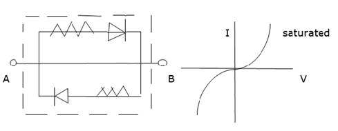
a)
According to Ist figure both diodes are in forward bias ![]()
and current is given as :
![]()
b) In this case (according to IInd figure) one diode is in forward bias while other is in reverse bias.
Thus,
![]()
And current is given as :
![]()
I = OA
c) In this case (figure III) both diodes are forward biased
Thus,
![]() and current is given as :
and current is given as :
![]()
d) In this case (figure IV) one diode is forward bias and other is reverse bias but they are in parallel and thus current passes through diode which forward bias.
![]()
![]()
Solution 26
a) In A1 current is o because diode is reverse bias and thus resistance is infinite.
b) In A2 current is given as :
![]()
![]()
Solution 27
a)
According to ![]() figure , both diodes are forward bias
figure , both diodes are forward bias
∴ Net resistance offered by diodes is O.
Now ![]()
Now,
![]()
![]()
b) According to IInd figure one diode is forward bias and other diode is reverse bias thus current will pass through diode which is forward biased.
Thus,
![]()
![]()
Solution 28
a)
![]()
![]()
![]()
I= 0.42A
b)
![]()
![]()
I= 0.16A
Solution 29
a)
b)
Solution 30
There are two cases:
a)
If ![]() ,
then diode is forward biased and resistance will be :
,
then diode is forward biased and resistance will be :
![]()
b)
If ![]() ,
then diode is reverse biased and resistance will be:
,
then diode is reverse biased and resistance will be:
![]()
Solution 31
We know,
![]()
![]()
![]()
![]()
Solution 32
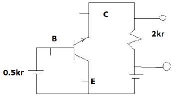
Now,
![]()
![]()
a)
change ![]()
![]()
![]()
Change in V = 8000v
b)
change in input voltage ![]()
![]()
=25mV
c)
Power gain ,![]()
![]()
![]()
Solution 33
![]()
a) X=1 ( if A = 1, B = 0, C=1)
b) X=0 (if A=B=C=1)
c) X=0 (if A=B=C=0)
Solution 34
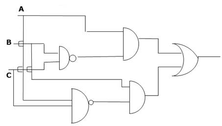
Circuit
diagram for ![]() is shown below :
is shown below :
Solution 35
To prove ![]()
a) If A=0
B=0
![]()
=0+1
=1
b) If A=0 B=1 or A=1 B=0
![]()
=0+1
=1
c) If A=1 B=1
![]()
=1+0
=1