CBSE Class 12-science Answered
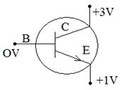
Action of n-p-n transistor
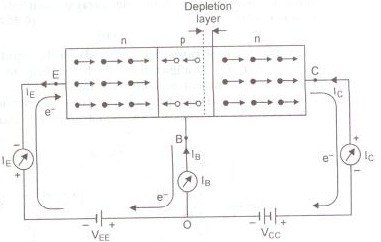
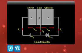
An NPN transistor is equivalent to two P-N junction diodes back to back with very thin P-regions connected together. The circuit diagram for the operation of NPN transistor is shown in fig. The two batteries VEE and VCC represent emitter supply and collector supply respectively. The emitter-base junction is forward biased and the base–collector junction is reverse biased. Consequently the internal potential barrier at emitter base junction neutralizes while the width of depletion layer at collector-base junction increases.
Base current and collector current : Under forward bias of emitter-base junction, the electrons in emitter and holes in base are compelled to move towards the junction, thus the depletion layer of emitter base junction is eliminated. As the base region is very thin, most electrons (about 98%) starting from emitter region cross the base region and reach the collector while only a few of them (about 2%) combine with an equal number of holes of base-region and get neutralized. As soon as a hole (in P-region) combines with an electron, a covalent bond of crystal atom of base region breaks releasing an electron-hole pair. The electron released is attracted by positive terminal of emitter battery VEE, giving rise to a feeble base current (IB). Its direction in external circuit is from emitter to base. The hole released in the base region compensates the loss of hole neutralized by electrons.
The electrons crossing the base and entering the collector, due to reverse biasing of collector-base junction, are attracted towards the positive terminal of collector battery VCC and enter the positive terminal of battery VEE. This causes a current in collector circuit, called the collector current. In addition to this the collector current is also due to flow of minority charge carriers under reverse bias of base-collector junction. This current is called the leakage current.
Thus collector current is formed of two components :
(i) Current (Inc), due to flow of electrons (majority charge carriers) moving from emitter to collector
(ii) leakage current (Ileakage) due to minority charge carriers, i.e., Ic= Inc + Ileakage
Emitter Current : When electrons enter the emitter battery VEE from the base causing base current or electrons enter the collector battery VCC from the collector causing collector current, an equal number of electrons enter from emitter battery VEE to emitter, causing the emitter current. The process continues.
Relation between Emitter, Base and Collector Currents :
Applying Kirchhoff's I law at terminal O, we get
IE = IB + IC
That is , the emitter current IE is the sum of base current IB and the collector current IC. This is the fundamental relation between currents in the bipolar transistor circuit.
Concept Videos
-
Transistors - Part 1
 This video explains the types of transistors and its action.
 -
Transistors - Part 2
 This video explains the action of a transistor in detail.
 -
Transistors - Exam Decoded
 This video contains practice questions on a transistor.