CBSE Class 12-science Answered
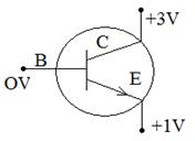
If the bias of the emitter-base junction of a transistor is sufficient to send a forward current and the collector base junction is reversed biased, the transistor is said to be in the active state.
The circuit diagram of a p–n–p transistor is as shown below:
A transistor when operated in the active state acts as an amplifier. The working of a common emitter transistor as an amplifier is based on the principle that a weak input signal given to the base region produces an amplified output signal in the collector region.
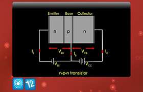
The circuit diagram for a p–n–p common emitter transistor amplifier can be drawn as shown below:
![]()
The battery VBB forward biases the emitter base junction and the battery VCC reverse biases the emitter collector region. The e.m.f. of the batteries should be greater than the barrier potential across base-emitter and collector emitter junction. The output current produces a potential difference across the load resistance RL. A weak alternating signal is applied between the base and the emitter. When the signal increases in the positive direction, the base current also increases. The base current is amplified b times and appears at the collector. The collector current flowing through the collector load resistance produces a voltage. This output voltage is equal to the collector current times the load resistance. Thus, an amplified output is obtained. The voltage gain = output voltage/input voltage.
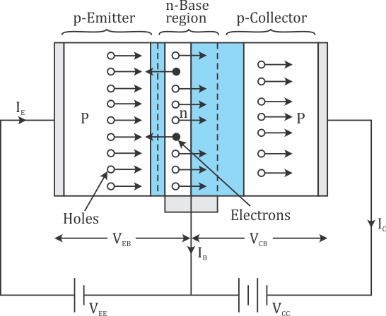
In a transistor, the base is thin and lightly doped so that it contains smaller number of majority carriers. This reduces the recombination rate of free electrons and holes in the base region when the majority carriers go from the emitter to the collector.
On the other hand, the emitter region in a transistor is heavily doped because the emitter supplies the majority carriers for the current flow.
Concept Videos
-
Transistors - Part 1
 This video explains the types of transistors and its action.
 -
Transistors - Part 2
 This video explains the action of a transistor in detail.
 -
Transistors - Exam Decoded
 This video contains practice questions on a transistor.