"The depletion region of unbiased pn junction contains only fixed ions".Sir, isn't this statement true?I've found in a mcqs book(arihant publications) that the depletion region of unbiased pn junction contains both es and holes. i got confused .please give me an answer sir.
Asked by Sumayya
16th January 2016,
7:23 PM
Answered by Expert
Answer:
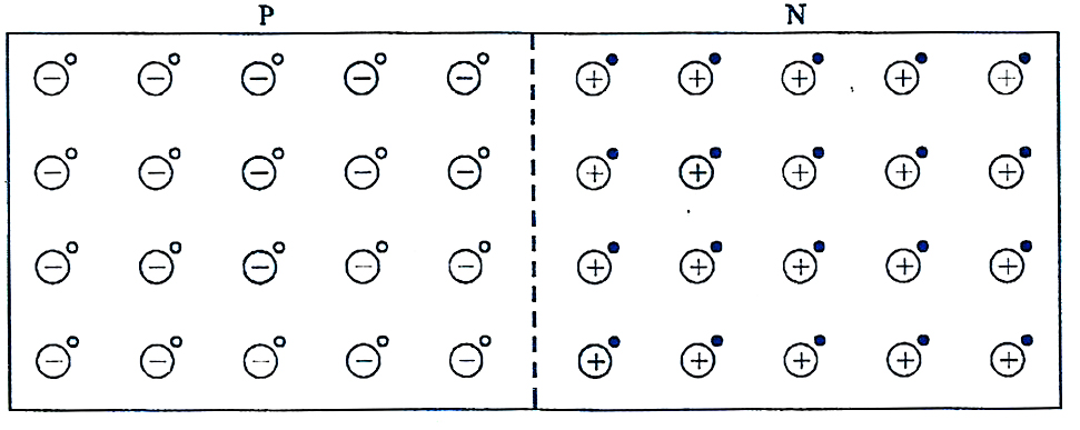
The P region has holes which are mobile (able to move) and negatively charged impurity ions which are immobile (not moving or motionless). The N region has positively charged impurity ions which are immobile and free electrons.
After PN junction diode has been formed, diffusion of holes begins from the P region to the N region. Similarly, the diffusion of electrons begins from the N region to P region. The holes and free electrons diffusing towards each other combine near the junction. Each recombination eliminates an electron and a hole. The net effect of such recombination is that the positive donor ions in N region and the negative acceptor ions in the P region in the neighbourhood of the junction are left uncompensated. Holes trying to diffuse into the N reion are repelled by uncompensated positive charge of the donor ions. Similarly, the electrons trying to diffuse into the P region are repelled by the uncompensated negative charges of the acceptor ions. The region containing the uncompensated acceptor and donor ions is called depletion region. This is because there is a depletion of mobile charges ( i.e., holes and free electrons) in the region. Since, this region contains only the immobile ions which are elctrically charged therefore, this region is called space-charge region.
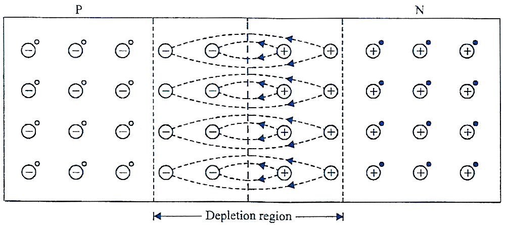
In the above fig., and electric field is set up between the donor and acceptor ions in the deplection region. The N side is at greater potential than the P side. The electrons of N side are at greater potential and thus are prevented to go to the lower potential of P side. Similarly, holes in P side find themselves at a lower potential and thus are prevented to cross the N side. Thus, there is a barrier at the junction which opposes the movement of majority charge carriers. The difference of potential from one side of the barrier to the other side is called potential barrier or height of the barrier. Its value is nearly 0.7 V for a silicon PN junction and 0.3 V for germanium diode.
Answered by Expert
17th January 2016,
3:21 PM
Rate this answer
- 1
- 2
- 3
- 4
- 5
- 6
- 7
- 8
- 9
- 10
You have rated this answer /10
Your answer has been posted successfully!
RELATED STUDY RESOURCES :
KERALA Class-12-science QUESTION ANSWERS
Browse free questions and answers by Chapters
- 1 Electric Charges and Fields
- 2 Electrostatic Potential and Capacitance
- 3 Current Electricity
- 4 Moving Charges and Magnetism
- 5 Magnetism and Matter
- 6 Electromagnetic Induction
- 7 Alternating Current
- 8 Electromagnetic Waves
- 9 Ray Optics and Optical Instruments
- 10 Wave Optics
- 11 Dual Nature of Radiation and Matter
- 12 Atoms
- 13 Nuclei
- 14 Semiconductor Electronics
- 15 Communication Systems
Trending Tags
Latest Questions
JEE Main Mathematics
Asked by amaladelsingh
28th October 2020,
10:24 PM
CBSE X Biology
Asked by reenacharan2008
28th October 2020,
9:11 PM