CBSE Class 12-science Answered
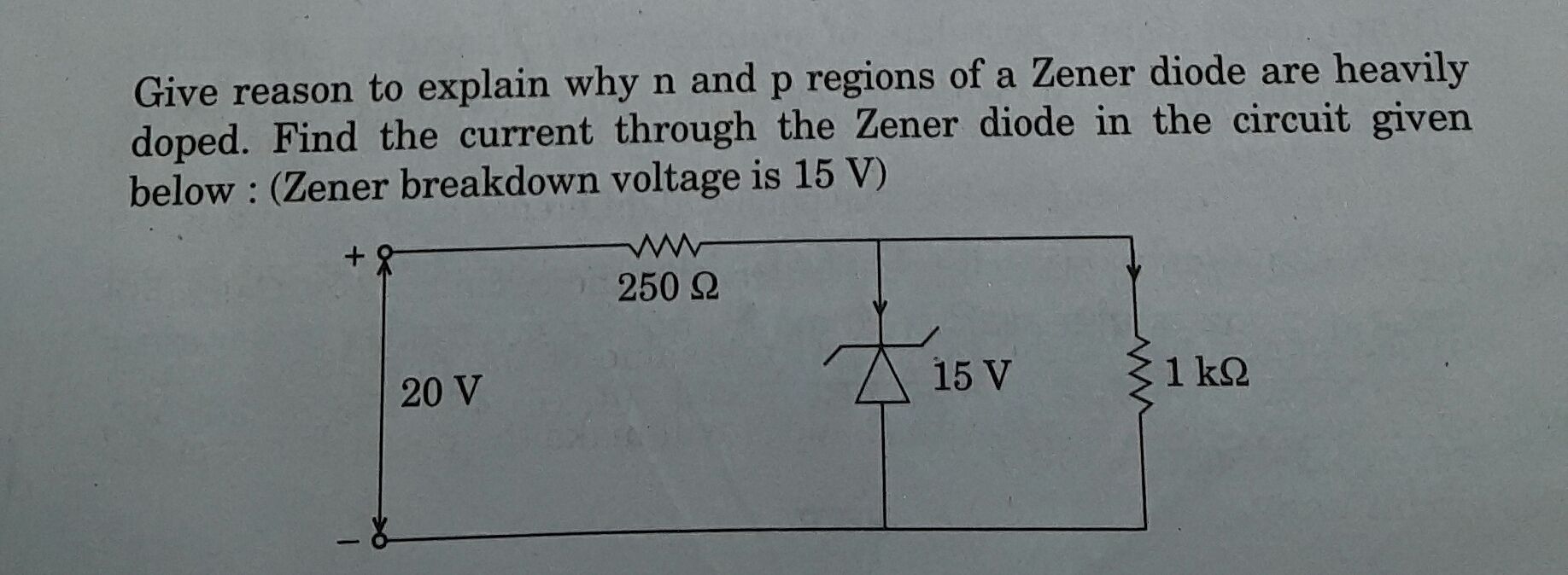
Zener diode is used for regulating the unregulated voltage supply.
In Zener diode, both p and n sides are heavily doped. Due to high dopant density, the depletion junction width is small and the junction field is high. Under large reverse bias, the high junction field may strip an electron from the valence band which can tunnel to the n side quantum mechanically through the thin depletion layer.
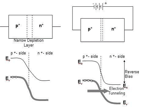
Fig (a) Unbiased p+-n+ junctions Fig (b) Reverse biased p+- n+ junctions of Zener diode
This takes place after a certain critical voltage is crossed, and is called 'internal field emission', which gives rise to a high reverse or 'breakdown' current. Such a breakdown is called 'Zener breakdown'.
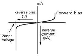
Fig (b) V-I characteristics of a Zener diode
After breakdown, a large current can be produced by an almost insignificant change in the reverse bias voltage. So, for widely different currents, the voltage across the Zener-diode stays constant. This leads it to be used in voltage regulation of DC voltages.
Concept Videos
-
Applications of p-n Diode - Part 1
 This video explains the diode in a forward and a reverse bias.
 -
PN diode application
 Diode V-I characteristics Diode as a rectifier Special purpose diodes.
 -
Applications of pn Diode
 Diode V-I characteristics Diode as a rectifier Special purpose diodes