CBSE Class 12-science Answered
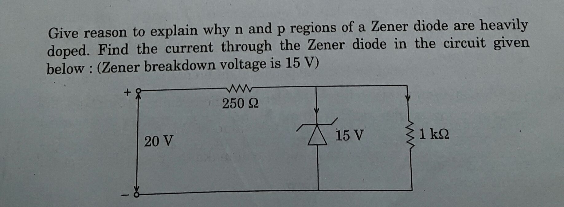
A Zener diode is fabricated by heavily doping both p and n sides of the junction. Because of heavy doping, a very thin (<10−6 m) depletion region is formed between the p and n sides, and hence, the electric field of the junction is extremely high (~5 × 10⁶ V/m) even for a small reverse bias voltage of about 5V.
Zener diode as a voltage regulator:
To get a constant d.c. voltage from the d.c. unregulated output of a rectifier, we use a Zener diode. The circuit diagram of a voltage regulator using a Zener diode is shown in the figure below.
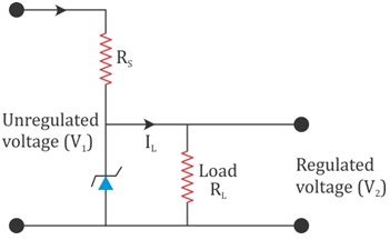
The unregulated d.c. voltage is connected to the Zener diode through a series resistance Rs such that the Zener diode is reverse biased. If the input voltage increases, the current through Rs and the Zener diode also increases. This increases the voltage drop across Rs without any change in the voltage across the Zener diode. This is because the Zener voltage remains constant in the breakdown region even though the current through it changes.
Similarly, if the input voltage decreases, the current through Rs and the Zener diode also decreases. The voltage drop across Rs decreases without any change in the voltage across the Zener diode. Thus, any increase or decrease in the input voltage results in an increase or decrease of the voltage drop across Rs without any change in the voltage across the Zener diode. Hence, the Zener diode acts as a voltage regulator.
Concept Videos
-
Applications of p-n Diode - Part 1
 This video explains the diode in a forward and a reverse bias.
 -
PN diode application
 Diode V-I characteristics Diode as a rectifier Special purpose diodes.
 -
Applications of pn Diode
 Diode V-I characteristics Diode as a rectifier Special purpose diodes