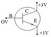
CBSE Class 12-science Answered
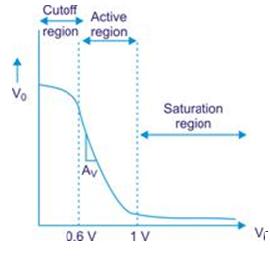
If we plot Vo Vs Vi , we get a graph as shown in figure; this characteristic curve is also called transfer characteristic curve of a base biased transistor in CE configuration.
The curve shows that there are three non-linear regions:
(i) between cut-off stage and active stage
(ii) between active stage and saturation stage;
For using the transistor as an amplifier we will use the active region of
the Vo versus V i curve. The slope of the linear part of the curve represents
the rate of change of the output with the input. It is negative because the
output is VCC - ICRC and not ICRC. That is why as input voltage of the CE
amplifier increases its output voltage decreases and the output is said to
be
out of phase with the input. If we consider ![]() Vo and
Vo and ![]() Vi as small
Vi as small
changes
in the output and input voltages then ![]() Vo/
Vo/ ![]() Vi is called the small
Vi is called the small
signal voltage gain AV of the amplifier.
If
the VBB voltage has a fixed value corresponding to the mid
point of the active region, the circuit will behave as a CE amplifier with
voltage gain ![]() Vo/
Vo/ ![]() Vi . We can express the voltage gain AV
in terms of the resistors in the circuit and the current gain of
the transistor as follows.
Vi . We can express the voltage gain AV
in terms of the resistors in the circuit and the current gain of
the transistor as follows.
We have, Vo= VCc - ICRC
Therefore,
![]() Vo = 0 - RC
Vo = 0 - RC ![]() IC
IC
Similarly, from Vi = IBRB+ VBE
![]() Vi =
R B
Vi =
R B ![]() IB +
IB + ![]() VBE
VBE
But
![]() VBE is negligibly small in comparison to
VBE is negligibly small in comparison to ![]() IBRB in this circuit.
IBRB in this circuit.
So, the voltage gain of this CE amplifier is given by
AV
=
- RC ![]() IC/ RB
IC/ RB ![]() IB
IB
=
- ![]() ac(RC /RB )
(14.14)
ac(RC /RB )
(14.14)
where
![]() ac is equal to
ac is equal to ![]() IC/
IC/ ![]() IB .
IB .
Thus the linear portion of the active region of the transistor can be exploited for the use in amplifiers.
Concept Videos
-
Transistors - Part 1
 This video explains the types of transistors and its action.
 -
Transistors - Part 2
 This video explains the action of a transistor in detail.
 -
Transistors - Exam Decoded
 This video contains practice questions on a transistor.