CBSE Class 12-science Answered
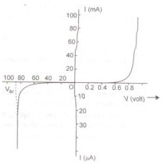 (i) Identify the semiconductor diode used.
(ii) Draw the circuit diagram to obtain the given characteristics of this diode.
(iii) Briefly explain how this diode can be used as a voltage regulator.
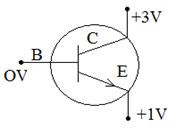
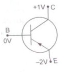
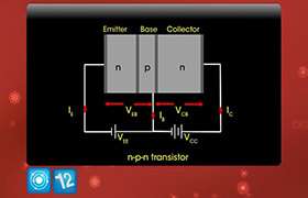
b) In the fig. given along side is (i) the emitter and (ii) the collector forward or reverse biased ?
(i) Identify the semiconductor diode used.
(ii) Draw the circuit diagram to obtain the given characteristics of this diode.
(iii) Briefly explain how this diode can be used as a voltage regulator.
b) In the fig. given along side is (i) the emitter and (ii) the collector forward or reverse biased ?
a)
(i) Semiconductor diode used is zener diode (but the voltage quoted in fig. are much less than actual values. Vbr is usually < 6 V)
(ii) The circuit diagram for reverse characteristics of Zener diode is shown fig.
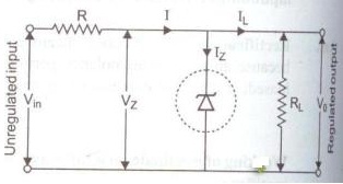
(iii) Zener diode as a voltage Regulator:
In the reverse breakdown region, the voltage across the zener diode remains constant, even if the current through zener diode increases considerably. The circuit diagram for a zener diode as voltage regulator is shown above. Here the zener diode is joined in reverse bias to the fluctuating d.c input voltage through resistance R of suitable value depending upon the zener voltage.The constant output is taken across a load resistance RL connected in parallel with zener diode.
When the input d.c voltage increases beyond a certain limit, the voltage across the zener diode becomes constant equal to zener break down voltage , but the current through the zener diode circuit rises sharply as the dynamic resistance of zener diode becomes almost zero, after zener breakdown voltage.Due to which there is an increase in voltage drop across R. Since RL is connected in parallel so the voltage across RL remains the same as that of zener break down voltage.Hence the output voltage remains constant.
b)The given transistor is p-n-p transistor. The emitter is reverse biased and the collector is forward biased.
Concept Videos
-
Transistors - Part 1
 This video explains the types of transistors and its action.
 -
Transistors - Part 2
 This video explains the action of a transistor in detail.
 -
Transistors - Exam Decoded
 This video contains practice questions on a transistor.