CBSE Class 12-science Answered
(a) We know that in an n-type semiconductor, the concentration of electrons is more compared to the concentration of holes. Similarly, in a p-type semiconductor, the concentration of holes is more than the concentration of electrons.
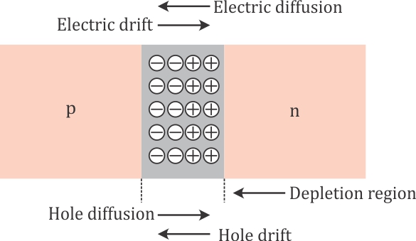
During the formation of a p–n junction and because of the concentration gradient across the p and n sides, holes diffuse from the p-side to the n-side (p → n) and electrons diffuse from the n-side to the p-side (n → p). This motion of charge gives rise to a diffusion current across the junction. When an electron diffuses from n → p, it leaves behind an ionised donor on the n-side. This ionised donor (positive charge) is immobile as it is bonded to the surrounding atoms. As the electrons continue to diffuse from n → p, a layer of positive charge (or positive space–charge region) on n-side of the junction is developed. Similarly, when a hole diffuses from p → n due to the concentration gradient, it leaves behind an ionised acceptor (negative charge) which is immobile. As the holes continue to diffuse, a layer of negative charge (or negative space–charge region) on the p-side of the junction is developed. This space–charge region on either side of the junction together is known as the depletion region.
Because of the positive space–charge region on the n-side of the junction and negative space charge region on the p-side of the junction, an electric field directed from the positive charge towards the negative charge develops. Due to this field, an electron on the p-side of the junction moves to the n-side and a hole on the n-side of the junction moves to the p-side. The loss of electrons from the n-region and the gain of electrons by the p-region cause a difference of potential across the junction of the two regions. This is how the barrier potential is formed.
(b)
(i) If a small voltage is applied to a p–n junction diode in the forward bias, then the barrier potential decreases.
(ii) If a small voltage is applied to a p–n junction diode in the reverse bias, then the barrier potential increases.
Concept Videos
-
p-n Diode - Part 1
 This video explains the basics of a pn junction.
 -
p-n Diode - Part 2 ...
 This video explains the working of a pn junction diode in forward and rever...
 -
PN Diode
 Study p-n junction, semiconductor diode, diode in forward and reverse bias...